Discover our primary catalog of high-density DRAM and performance server units designed to power modern cloud networks.

As computational demands scale exponentially with the rise of Large Language Models (LLMs), deep learning networks, and multi-tenant cloud ecosystems, the global server DRAM industry has transformed. Server RAM is no longer viewed merely as temporary data storage. Instead, it serves as one of the critical architectural components determining execution speed, overall system efficiency, and thermodynamic management within enterprise-level infrastructures.
Modern servers utilize complex multi-channel memory controller designs to support dozens of cores per socket. In high-performance environments (such as Intel® Xeon® Scalable and AMD EPYC™ architectures), memory bandwidth per core represents a vital performance limiting factor. Consequently, enterprise system planners must carefully evaluate the shift from legacy standards (like low-frequency DDR3 or standard DDR4) to next-generation DDR5 and emerging Compute Express Link (CXL) paradigms. The demand for massive throughput in applications like the DeepSeek training frameworks requires memory systems that offer not only dense architectures but also high reliability under continuous workload stress.
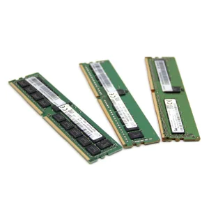
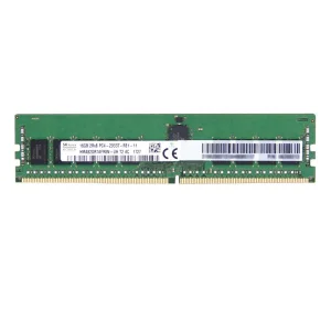
For procurement professionals, understanding memory configurations requires examining complex physical technicalities. Our manufacturing methodology targets the core parameters of advanced server DRAM architectures. From 288-pin DDR4 form factors operating at stable 1.2V configurations with low latency (0.625ns timing intervals) to high-speed DDR5 standards with on-board PMIC (Power Management Integrated Circuits), we design modules that minimize signal attenuation and maximize data reliability across all target workloads.
Enterprise server memories differ significantly from consumer-grade desktop or laptop RAM. Datacenters require continuous, uninterrupted runtime (often targeting 99.999% availability). To achieve this level of performance, server DRAM integrates hardware-level features designed to guarantee data integrity, manage heat, and prevent random bit-flip errors.
ECC memory continuously detects and corrects single-bit memory errors. By utilizing a specialized algorithm and reserving extra memory bits (72-bit bus width instead of 64-bit), ECC helps prevent system crashes, blue screens, and data corruption in high-volume transaction servers.
RDIMMs contain a hardware register between the system's memory controller and the DRAM modules. This register buffers command and address signals, reducing the electrical load on the memory controller and allowing systems to support a greater number of memory ranks per channel.
LRDIMMs replace the register found in standard RDIMMs with a memory buffer chip. This buffer reduces both the electrical command loads and data line loads. As a result, datacenters can deploy maximum-density memory configurations without sacrificing operating frequencies.
Furthermore, reliability, availability, and serviceability (RAS) features represent the baseline requirements for modern virtualization platforms. With Advanced Single-Device Data Correction (SDDC), also known as Chipkill, servers can withstand the complete failure of a physical memory chip on a module without causing system downtime or corrupted outputs. In tandem with memory-mirroring and hot-spare configurations, our modules offer multi-layered hardware protection for enterprise servers running demanding databases and virtual environments.
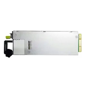
Integrating specialized GPU computational capacity with robust enterprise system memory configurations.
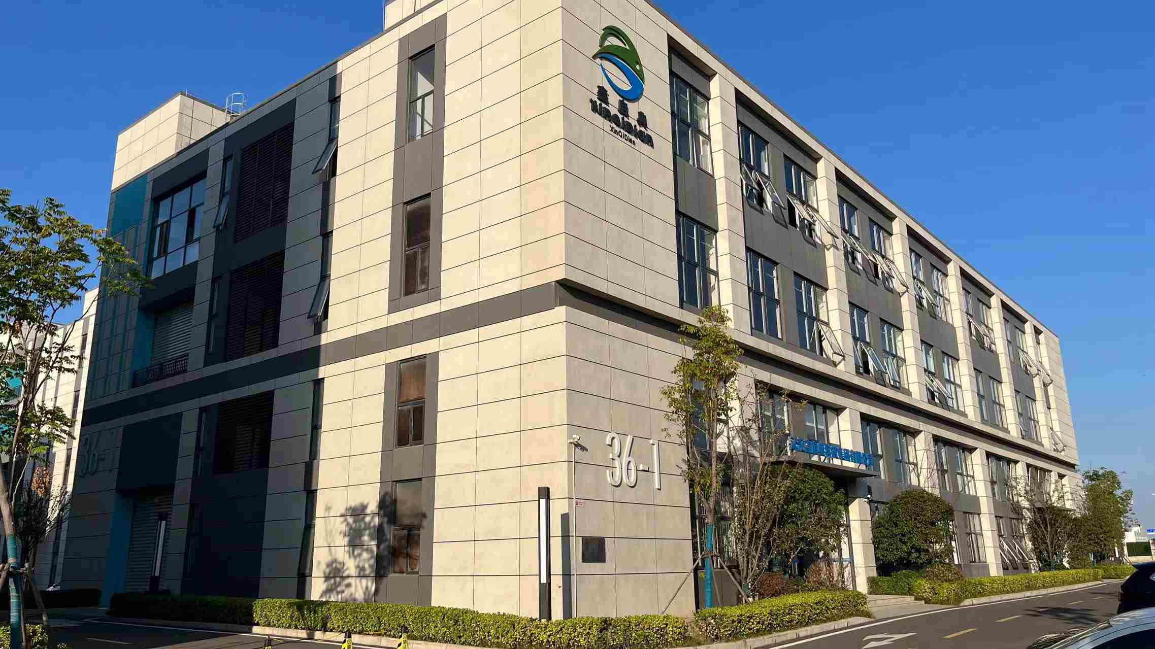
NexaGPU is a professional AI GPU server manufacturer and supplier specializing in high-performance computing infrastructure, GPU clusters, and customized AI server solutions for global enterprises, data centers, and AI development companies. Established in 2016, NexaGPU has rapidly grown into a trusted provider of advanced GPU computing systems. The company operates a modern manufacturing facility with a building area of approximately 320㎡, supporting efficient production, assembly, and testing of AI server systems.
Our operation is built on deep integration with upstream silicon chip vendors, memory dies producers, PCB board developers, and thermal component creators. By partnering with over 850 industry supply chain leaders, NexaGPU ensures that every memory module and server unit integrates top-tier components. We source and process components to assemble robust systems, helping to protect your investments from unpredictable market constraints.
Additionally, our high-density R&D team (comprising 120 dedicated engineers) designs and validates server storage architecture, GPU integration interfaces, and advanced liquid cooling designs. Over the past fiscal year alone, our facility designed and deployed 85 new product models, supporting diverse platforms from low-latency AI inference nodes to high-density GPU computing clusters.
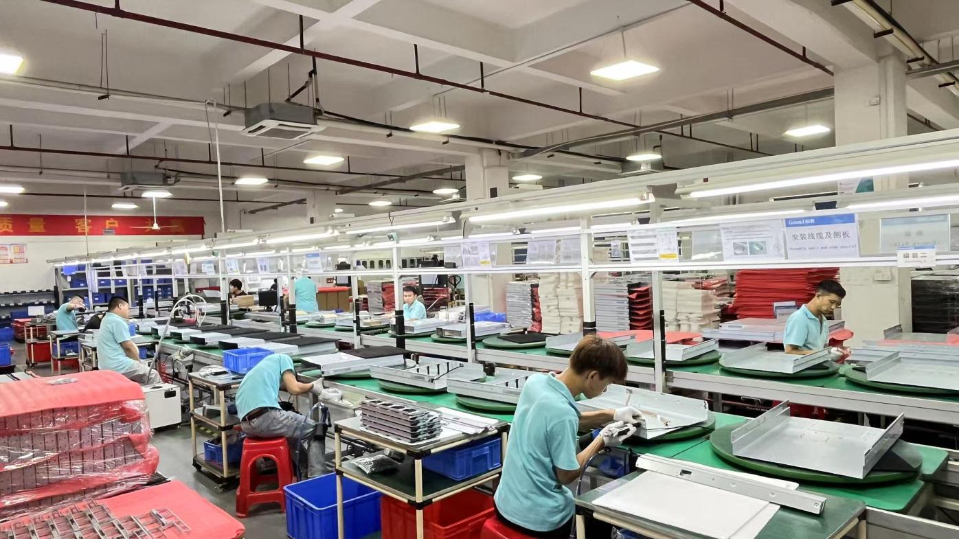
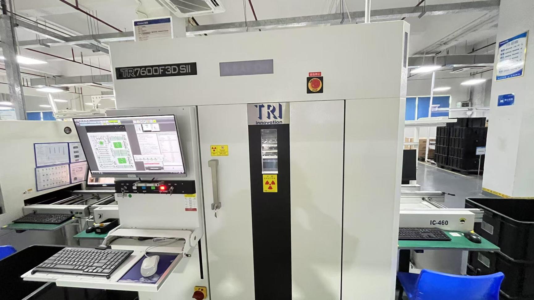
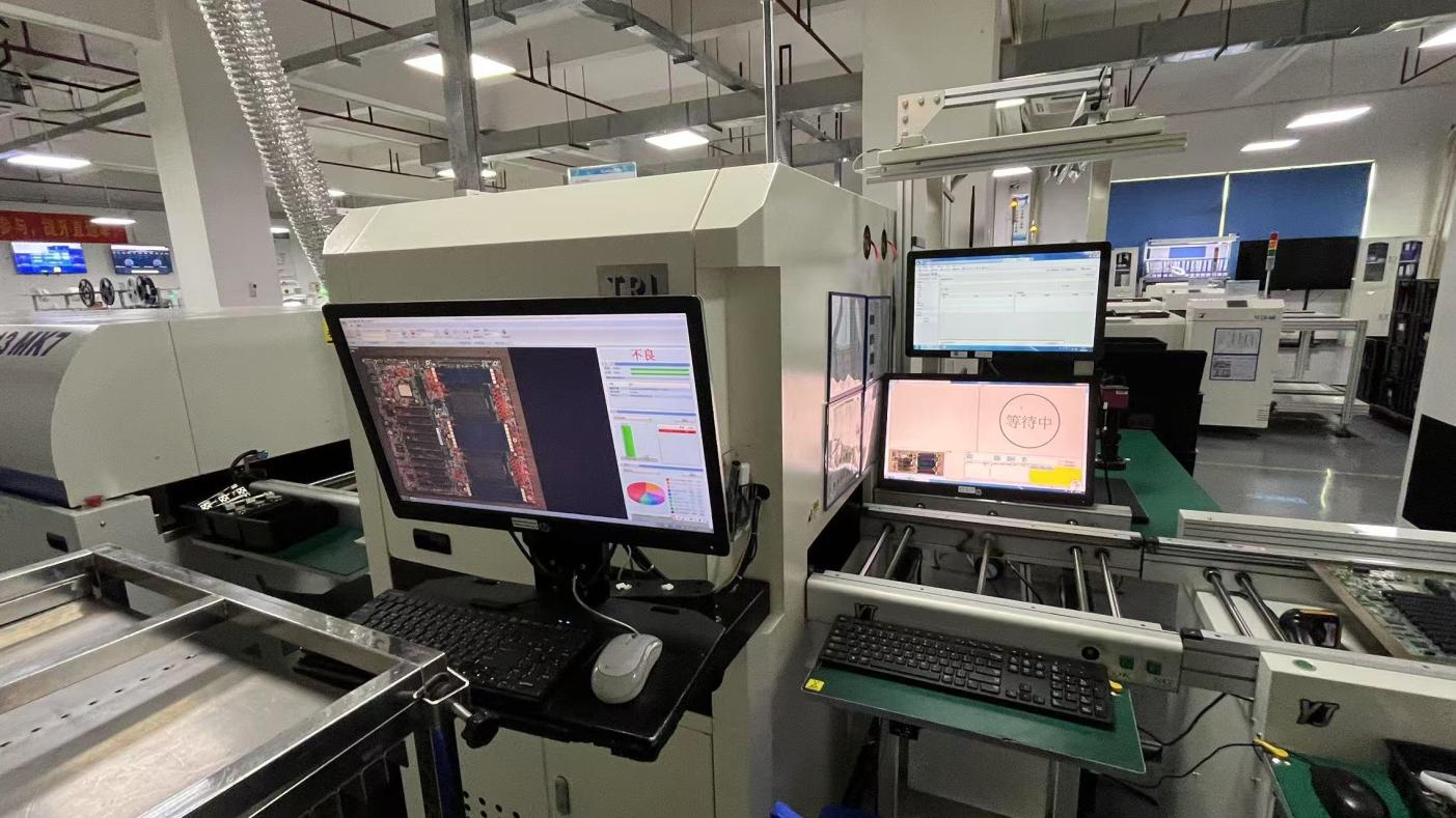
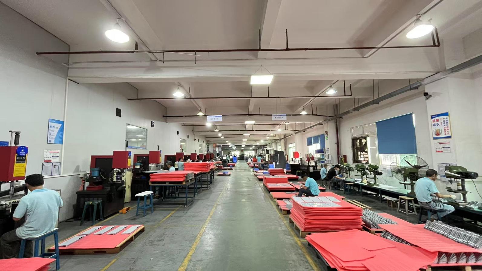
Below are real-world captures of our manufacturing floor, testing labs, and distribution logistics networks, showcasing our commitment to high industry standards:
Modern server RAM applications extend far beyond centralized cloud data hubs. Increasingly, deployment occurs in Edge Computing Nodes and harsh industrial environments. These localized deployments face unique challenges: high thermal variations, structural vibrations, and dust exposure, all while requiring high-speed data processing close to the point of generation.
For example, in automated manufacturing lines, high-frequency sensors generate gigabytes of telemetry data per second. High-density RAM configurations allow Edge AI servers to process this data locally for real-time quality control, avoiding the latency and security concerns of routing it to a central cloud server. In these settings, standard memory modules can fail due to thermal fatigue or electrochemical migration on the PCB. That is why our industrial-grade server RAM options utilize thicker conformal coatings, underfills, and gold finger contacts (up to 30 micro-inches) to ensure long-term durability and consistent signal transmission.
Additionally, telecommunications networks depend on ruggedized edge units to route high-volume traffic. 5G infrastructure, network function virtualization (NFV), and real-time content delivery networks (CDNs) require memory modules that combine high density with low power usage. Operating at lower voltages (like 1.2V for DDR4 and 1.1V for DDR5) helps decrease the overall power footprint of remote edge stations, improving system reliability in off-grid or solar-powered telecom installations.
For international enterprise procurement, meeting stringent compliance and quality standards is critical. Because server memory failure can disrupt operations and lead to financial losses, NexaGPU implements strict validation procedures throughout the production lifecycle.
To support this commitment to quality, NexaGPU utilizes a specialized team of 45 QC specialists. These engineers carry out detailed inspection phases, including:
Every batch of memory modules undergoes testing inside controlled environmental chambers. These modules run intensive memory tests at temperatures ranging from -40°C to 85°C to confirm they meet thermal expansion tolerances.
Using advanced testers, we verify the write/read margins and timing parameters of every pin on our 288-pin DDR4 and DDR5 modules, ensuring stable operation at rated speeds like 3200MHz.
Before leaving the factory, our memory modules are installed in active server systems (such as Dell PowerEdge and FusionServer racks) and run under 100% compute load for 24 to 72 hours to prevent early failures.
Our production lines conform to CE, FCC, RoHS, and WEEE requirements. This ensures our products meet safety standards and environmental regulations for deployment in North America, Europe, and Asia.
As CPU core counts continue to rise, traditional memory buses face physical limits in terms of board space and pin count. This constraint has led the server industry toward Compute Express Link (CXL)—an open-industry standard interconnect built on the PCIe physical layer. CXL enables high-speed, low-latency communication between processors, accelerators, and memory devices.
Under the CXL architecture, memory is no longer restricted to a dedicated motherboard socket. Instead, CXL allows memory pooling, where multiple servers can share access to a central pool of memory. This architecture helps reduce underutilized memory capacity in datacenters and allows resource allocation to be adjusted dynamically based on changing workload requirements.
By using CXL-based memory expansion, datacenters can scale their memory capacities beyond standard limits. This capability is useful for large in-memory databases, real-time analytics engines, and the complex training workloads required by modern AI tools. As a result, systems can run larger datasets and models on fewer nodes, helping to lower initial hardware costs and reduce power consumption.
Detailed answers to frequent technical inquiries from enterprise datacenter engineers and procurement managers.
RDIMMs feature a register chip that buffers only address and command lines, leaving the data signals connected directly to the memory controller. This design offers low latency at lower capacities. LRDIMMs, on the other hand, use a buffer chip to isolate both control and data lines. This isolation lowers electrical loads, allowing you to install higher-capacity modules and populate more slots per channel, though it may introduce a small latency trade-off.
ECC (Error-Correcting Code) memory uses parity bits to identify and correct single-bit errors in real time. If an uncorrectable multi-bit error occurs (which is rare but possible under high load), the memory system detects the error and alerts the operating system. In virtualized and database environments, this trigger prevents data corruption by initiating a controlled system halt or kernel panic rather than continuing with corrupted data.
DDR5 operates at a lower base voltage (1.1V) compared to DDR4 (1.2V), which reduces power use under standard loads. Additionally, DDR5 moves power management from the motherboard to the module itself using an onboard Power Management Integrated Circuit (PMIC). While this change improves power efficiency and voltage regulation, it concentrates heat generation on the memory module, requiring server chassis designs with adequate airflow and thermal management.
Most server architectures allow you to mix memory capacities across different channels, provided they follow the manufacturer's specific slot-population guidelines. However, mixing capacities on the same channel is generally not recommended. If you install modules with different operating speeds, the system will run all modules at the speed of the slowest installed unit. Mixing RDIMMs and LRDIMMs on the same motherboard is not supported.
DDR5 modules feature "on-die ECC," which corrects single-bit errors within the DRAM chip itself before sending the data to the CPU. This feature helps improve yield rates for higher-density memory chips. On-die ECC does not replace traditional system-level ECC, which checks and corrects errors along the data bus between the memory module and the CPU. Enterprise DDR5 modules combine both on-die ECC and system-level ECC to provide multi-layered data protection.
CAS (Column Address Strobe) Latency indicates the delay between the memory controller requesting data and the memory module returning it. For database systems and transactional workloads, lower latency helps improve performance. However, for bandwidth-heavy workloads like AI training or media rendering, high clock speeds and data throughput are often more important than raw CAS latency.
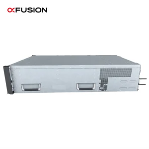
Browse our selection of enterprise-grade server barebones, storage racks, and custom computing nodes.