Demystifying the hardware demands of large language model (LLM) training, multi-modal alignment, and massive-scale gradient descent operations.
The exponential escalation of AI parameter counts—ranging from dense models to sparse Mixture of Experts (MoE) like DeepSeek-V3 and DeepSeek-R1—has reshaped the requirements of high-performance computing (HPC). Standard CPU architectures are no longer sufficient to process modern deep learning iterations within realistic timelines. Next-generation AI training systems demand specialized, high-density GPU acceleration frameworks, ultra-low latency optical interconnect architectures, and robust cooling technologies capable of dissipating high thermal design power (TDP).
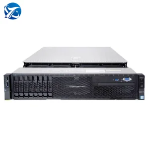
As a premier supplier in the enterprise GPU computing sector, NexaGPU engineers hardware configurations tailored to these demands. Operating since 2016 and backed by over 11 years of industry experience in high-performance server architecture, our hardware integrates high-bandwidth memory (HBM3e/HBM4), PCIe Gen 5.0 multiplexing, and advanced NVLink/NVSwitch networking configurations to eliminate compute bottlenecks.
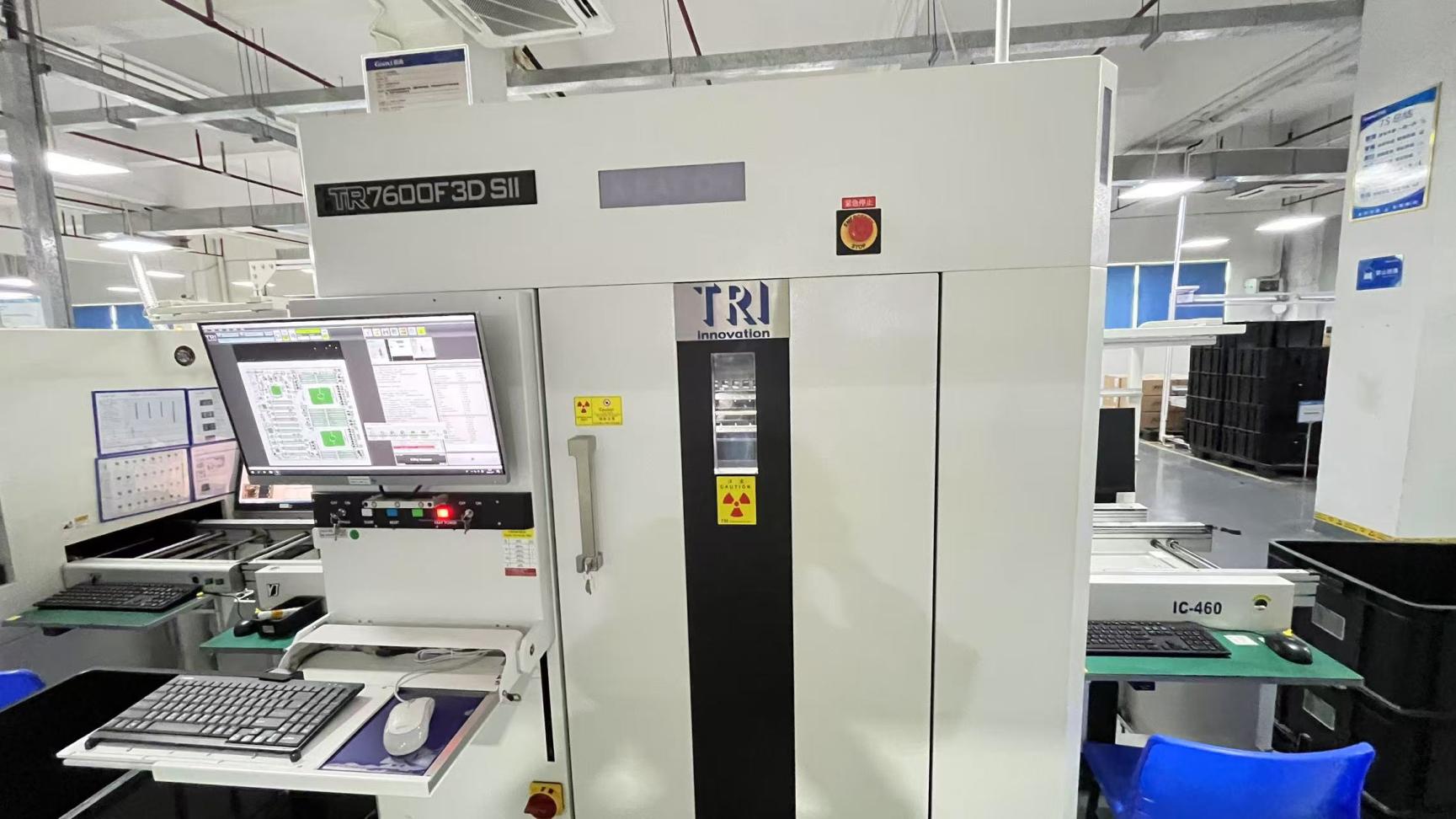
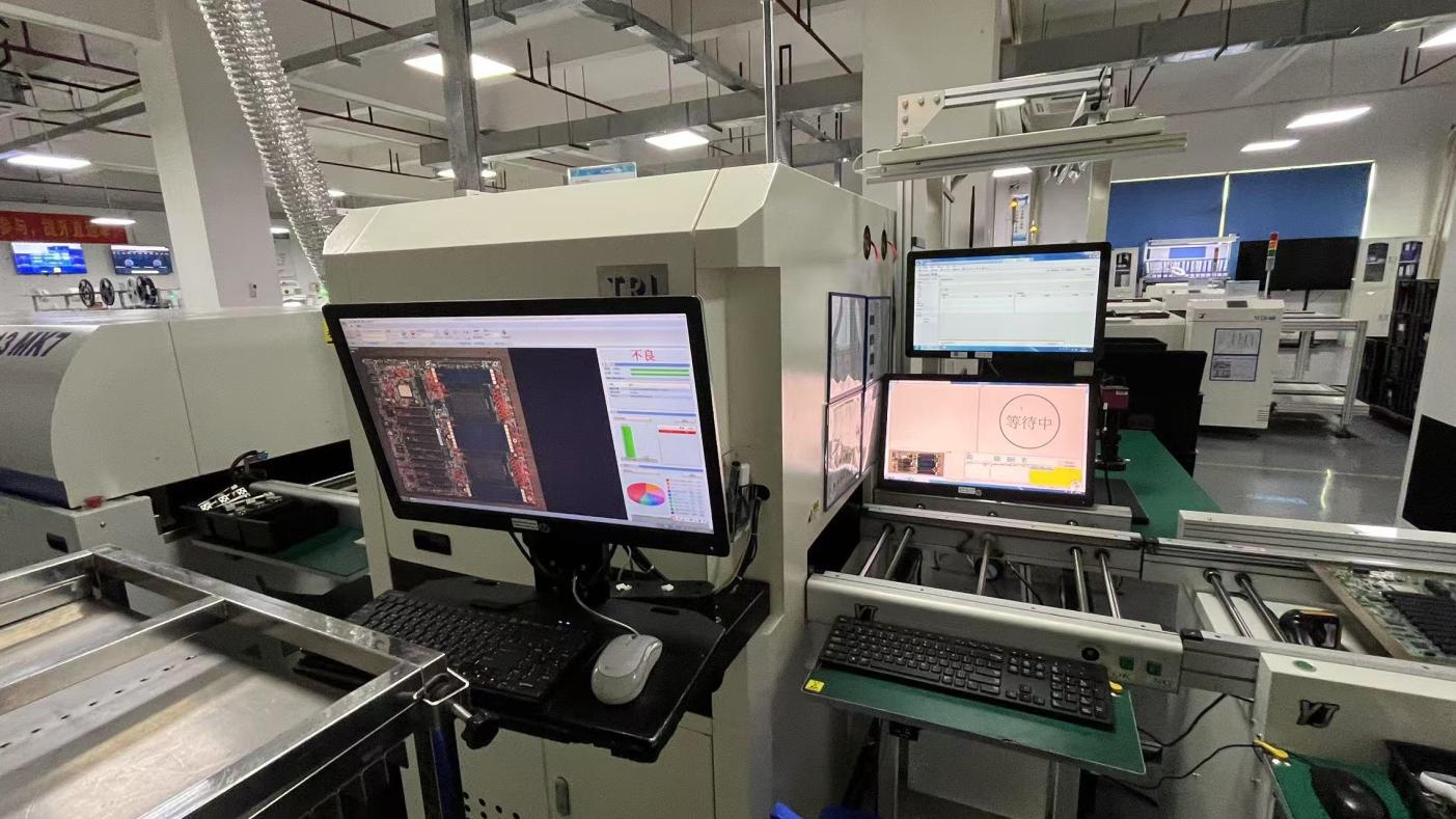
To maintain structural reliability under sustained 100% workloads, our products undergo a strict multi-stage inspection process. Managed by our internal team of 45 dedicated quality assurance (QC) specialists, every system undergoes 72-hour thermal stress testing, full PCIe signal integrity diagnostic scans, and high-throughput memory validation before shipment.
Engineering scalable pathways toward Zettaflop-scale computing, liquid cooling optimization, and optical hardware integration.
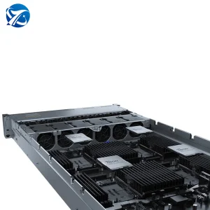
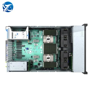
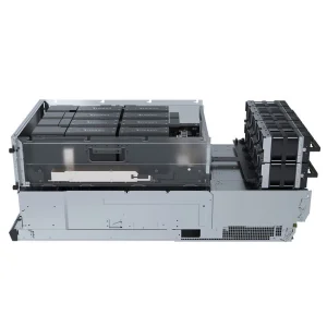
The technology roadmap of AI training systems is defined by the physical limits of semiconductor fabrication and thermal dissipation. As silicon processes approach atomic limits, scaling computing performance requires cluster-level scaling rather than single-chip enhancements. The design of our GPU rack nodes relies on high-bandwidth PCIe Gen 5 routing topologies and high-speed OAM (OCP Accelerator Module) form factors to optimize chip-to-chip bandwidth.
Looking forward, next-generation platforms will transition to PCIe Gen 6.0 and integration of CXL (Compute Express Link) protocols. This advancement allows dynamic memory sharing between host processors and GPU accelerators, mitigating out-of-memory errors during the loading of larger training datasets.
Furthermore, optimizing hardware for open-source AI architectures (such as DeepSeek and LLaMA) requires customizing compute setups. High-speed NVMe storage systems configured with hardware-level RAID arrays, powered by cards like the XC470C-M-8i SAS/SATA 12Gb/s card, ensure data pipelines are filled continuously, minimizing GPU idle times during training epochs.
With GPU power draw exceeding 700W to 1000W per accelerator, we are transitioning from standard high-CFM air-cooling to hybrid Direct-to-Chip (D2C) liquid cooling loops, optimizing PUE down to 1.15.
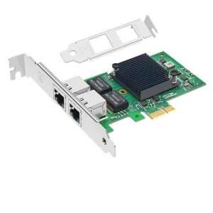
Integrating PCIe Gen5 switches, 800Gb/s InfiniBand, and RoCEv2 network interface cards (NICs) to facilitate distributed training across thousands of concurrent nodes.
Leveraging the Shenzhen tech ecosystem, vertical component integration, and advanced structural quality control.
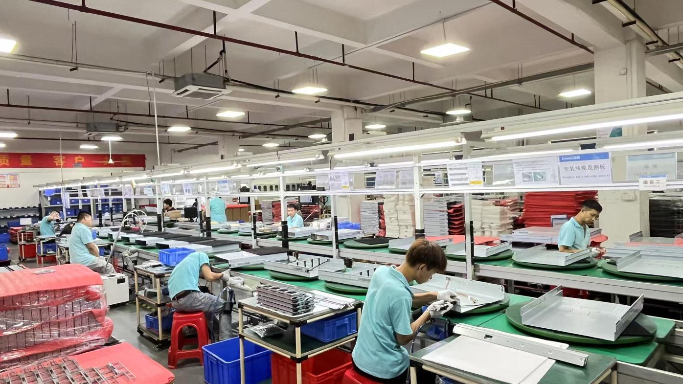
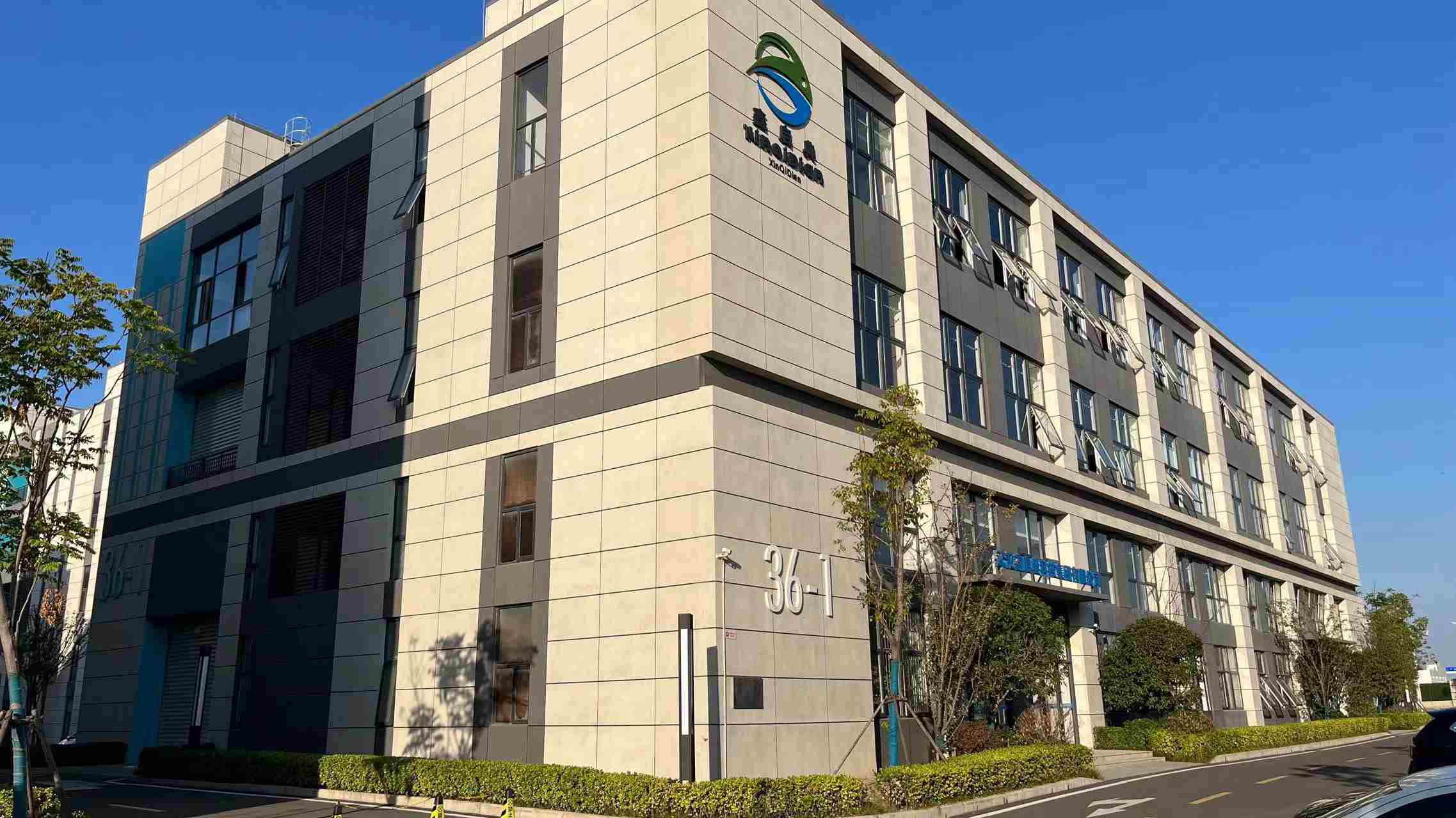
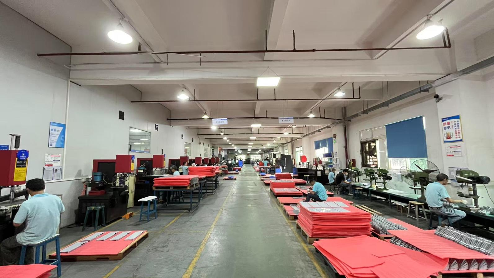
China's dominance in the global electronics supply chain is driven by structural efficiencies, co-located component ecosystems, and deep manufacturing expertise. NexaGPU's primary facility, located in the high-technology manufacturing hub of Shenzhen, China, utilizes an optimized 320㎡ layout configured for final system assembly, precision sensor integration, firmware flashing, and thermal-chamber testing.
By working closely with over 850 supply chain partners—ranging from PCB fabrication houses to alloy enclosure extruders—we reduce lead times compared to Western assembly lines. Components like the chassis, copper cold plates, and power distribution boards are sourced locally. This localized supply chain minimizes transit times and insulates client projects from delays caused by global shipping backlogs.
Our 45 QC specialists execute a 45-point testing protocol checking voltage ripple, storage performance, and memory error correction codes (ECC) under 100% system utilization.
Our facility hosts 120 R&D engineers specializing in signal integrity simulations and BIOS/IPMI customization, helping us launch 85 new product configurations over the past year.
With 6 years of international export experience, we handle customs clearance and documentation for direct delivery to North America, Europe, Southeast Asia, and the Middle East.
Deploying optimized computing infrastructure across high-impact vertical applications.
Processing sensor streams, high-definition mapping data, and training convolutional vision models. Requires high-throughput storage bandwidth to ingest petabytes of drive data.
Accelerating genomic alignment, protein folding models, and 3D medical scan segmentation. Configured with ECC memory arrays to prevent bit-flips during long training runs.
Running high-frequency risk simulations, multi-agent trade modeling, and time-series analysis using highly parallelized CPU/GPU architectures.
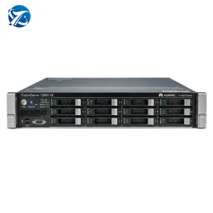
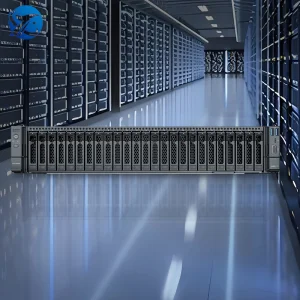
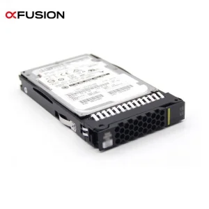
Each sector demands specific storage and network configurations. In autonomous driving, high-throughput SSD arrays (using platforms like our se005 Series 2.5 Inches SATA SSDs) are critical to ensure that data loaders do not starve the accelerators. In quantitative finance, compute density is prioritized, making 1U dual-socket setups like the FusionServer 1288H V5 suitable for low-latency calculations.
Our integration environment in Shenzhen features specialized diagnostics, testing racks, and assembly bays.
Mitigating global supply risk, navigating international trade frameworks, and ensuring operational SLA compliance.
Procuring high-performance computing hardware globally requires navigating international compliance standards. As an established exporter, NexaGPU ensures that all systems destined for international markets comply with target regulatory requirements, including CE, FCC, RoHS, and UL standards.
We provide custom packaging design using high-density polyethylene (HDPE) foam inserts, reinforced outer flight cases, and moisture-barrier vacuum packaging. This prevents physical acceleration shocks or humidity spikes from affecting system components during transit.
To maintain hardware uptime, NexaGPU provides spare parts packages (including fans, power supplies, and storage drives) with critical deployments. This allows local onsite engineers to perform repairs without waiting for international shipments.
Technical answers to key infrastructure questions from CTOs, system administrators, and infrastructure procurement managers.
For standard custom configurations using active motherboards and GPU models, our production and integration cycle requires 10 to 15 business days. Mass production of custom chassis designs or liquid-cooling loops may require 25 to 35 business days.
Our 45-person QA team executes a multi-stage testing protocol. This includes 24 hours of GPU stress testing (using workloads like FurMark and proprietary CUDA test suites), 24 hours of memory test loops (to check ECC functionality), and 24 hours of thermal stress validation.
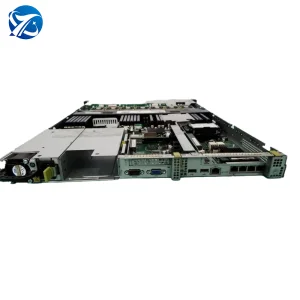
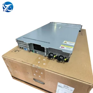
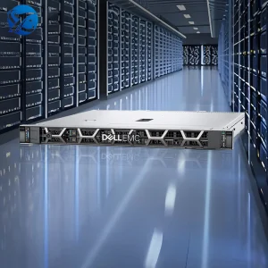
Yes. Our server systems, including the FusionServer G8600 V7 and custom xFusion systems, are compatible with primary training frameworks, including PyTorch, TensorFlow, JAX, DeepSpeed, and Megatron-LM, and support modern open-source models like DeepSeek-R1 and LLaMA.
We export under Incoterms including EXW, FOB, and CIF. We provide detailed export documentation, including Certificate of Origin and HS code classifications, to ensure customs processing in North America, Europe, Southeast Asia, and the Middle East.
Yes, our engineering team designs and manufactures direct-to-chip (D2C) cold plates and quick-disconnect couplings. We also offer CDU (Cooling Distribution Unit) optimization to fit standard datacenter power-density envelopes.